NIT Raipur inaugurates one-week SERB sponsored workshop on semiconductor devices.
2 min read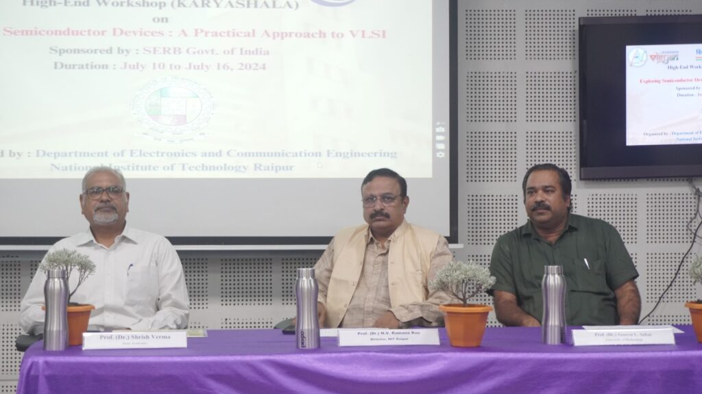
Raipur (Team Newsbuddy): National Institute of Technology (NIT) Raipur’s Department of Electronics & Communication Engineering (ECE) is organising a One-Week High-end workshop sponsored by SERB on “Exploring Semiconductor Devices: A Practical Approach to VLSI” from 10th to 16th July 2024. The Chief Patron of the workshop is Prof. (Dr.) N.V. Ramana Rao, Director, NIT Raipur. Patrons include Dr. Shrish Verma, Dean (Academics), Dr. Prabhat Diwan, Dean (R&C) and Dr Shubhojit Ghosh, Chairman, CEC. Chairman for the workshop is Dr. Toshanlal Meenpal, HoD, ECE. The workshop coordinators are Dr. G.P.S.C. Mishra and Dr. Ashish Kumar, ECE.
The inaugural ceremony for the workshop was held on 10th July, featuring Chief Guest Dr. N.V. Ramana Rao and Guest of Honor Prof. (Dr.) Samrat L. Sabat, University of Hyderabad. Dr. Shrish Verma, Dean (Academics), Dr. D. Sanyal, Dean (Faculty Welfare), Dr. Sameer Bajpai, Head, CDC, Dr. B. Acharya, HoD (I/C), ECE, faculty members, scholars, participants were present in this event.
In his address, Dr. Verma recalled the department’s journey from its transformation from GEC to NIT in 2005 and ECE Departments achievements despite limited resources. He briefed about the workshop’s objectives while guiding all participants on what they could learn from it. Dr. Rao highlighted the applications of semiconductors in solar panels, battery panels, etc., and discussed the bright future of this field in the country. Dr. Samrat emphasized the need for good designers for sustainable growth and explained the link between devices, circuits, and systems. He also stated that semiconductors are in high demand for sustainable growth and praised the Indian government’s investment in this sector. At last, Dr. Acharya proposed a vote of thanks and congratulated participants from different parts of the country for joining this workshop.
This one-week workshop will introduce participants to semiconductor devices and their practical applications through VLSI design. Participants will be able to learn about semiconductor physics, device optimization, fabrication techniques and VLSI design methods through hands-on experience as well as oral knowledge and interactive discussions.